- 您现在的位置:买卖IC网 > Sheet目录2011 > MAX5893EGK+D (Maxim Integrated Products)IC DAC 12BIT DUAL 500MSPS 68-QFN
MAX5893
tionship and detects if the phase drifts more than ±1
data clock cycle. If this occurs, the synchronizer auto-
matically reestablishes synchronization. However, dur-
ing the resynchronization phase, up to 8 data words
may be lost or repeated.
Bit 2 of register 02h disables or enables (default) the
automatic data clock phase detection. Disabling the
data synchronization circuitry requires the data clock
and the DAC clock phase to be locked.
DATACLK Modes
The MAX5893 has a main DATACLK available at
pin 14. An alternate DATACLK is available at pin 27
(DATACLK/B10) when configured in single-port data
input mode (bit 5, address 02h). The DATACLK can be
configured to accept an input clock signal for latching
the input data, or to source a clock signal that can drive
up to 10pF load while latching the input data (bit 3,
address 02h). If DATACLK is configured as an output, it
is frequency divided from the CLKP/CLKN input,
depending on the operating mode, see Table 4.
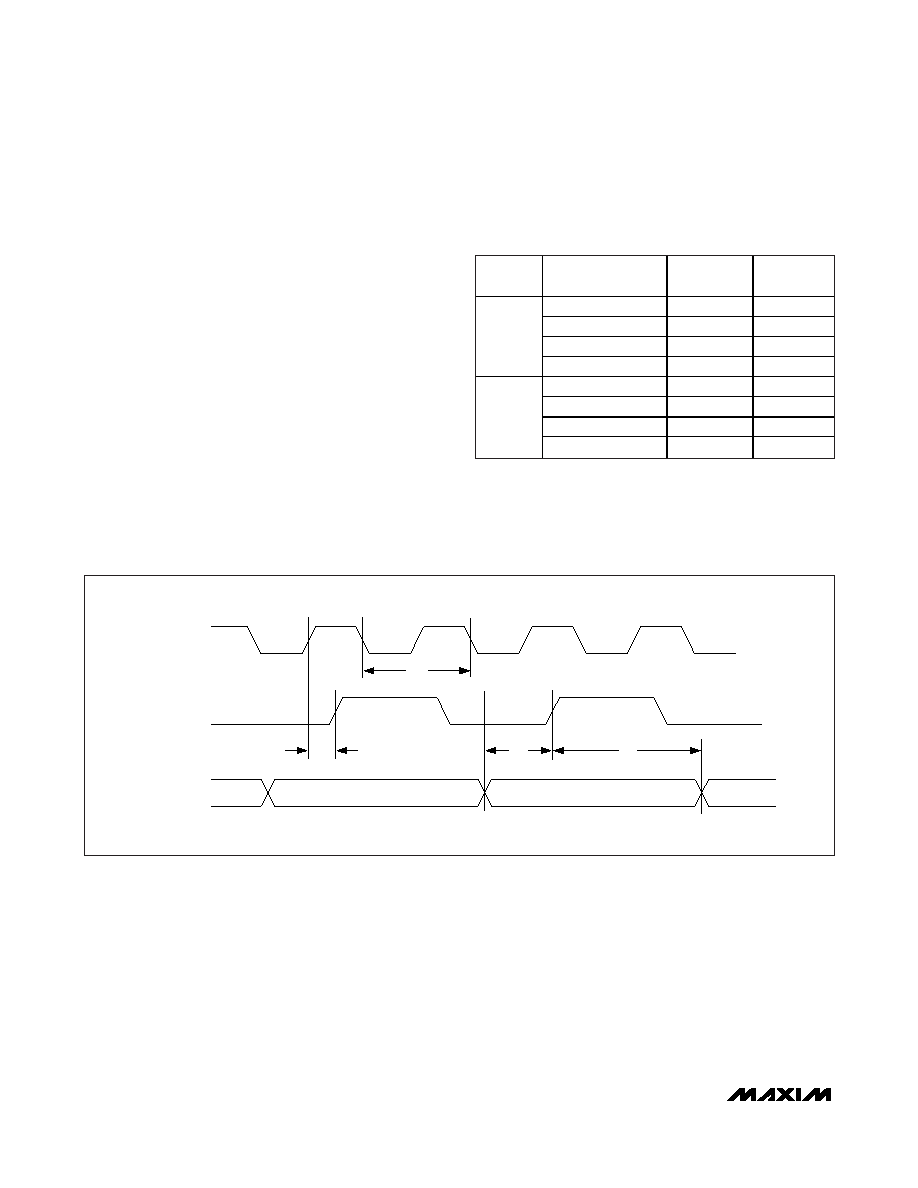
The MAX5893 can be configured to latch the input
data on either the rising edge or falling edge of the
DATACLK signal (bit 4, address 02h). Figure 4 shows
the timing requirements between the DATACLK signal
and the input data bus with latching on the rising edge.
12-Bit, 500Msps Interpolating and Modulating
Dual DAC with CMOS Inputs
18
______________________________________________________________________________________
INPUT
MODE
INTERPOLATION
RATE
fDATA:fCLK
fDAC:fCLK
1x
1:1
1:2
2x
1:1
4x
1:2
1:1
Single
Port
8x
1:4
1:1
1x
1:1
2x
1:2
1:1
4x
1:4
1:1
Dual Port
8x
1:8
1:1
Table 4. Clock Frequency Ratios in
Various Modes
Figure 4. Data Input Timing Diagram
tD
tDS
tCLK
CLKP–CLKN
DATACLK
A0–A11/B0–B11
tDH
发布紧急采购,3分钟左右您将得到回复。
相关PDF资料
MAX5894EGK+D
IC DAC 14BIT DUAL 500MSPS 68-QFN
MAX5895EGK+D
IC DAC 16BIT 500MSPS DUAL 68-QFN
MAX5898EGK+D
IC DAC 16BIT DUAL 500MSPS 68-QFN
MAX6900ETT+T
IC RTC I2C COMPAT 6-TDFN
MAX6902ETA+T
IC RTC SPI COMPAT 8-TDFN
MAX7375AXR604+T
IC OSC SILICON SC70-3
MAX7394ATTLY+T
IC OSC SILICON 922KHZ 6-TDFN
MAX7403CSA+
IC FILTER LOWPASS 8-SOIC
相关代理商/技术参数
MAX5893EGK+TD
功能描述:数模转换器- DAC 12-Bit 2Ch 500Msps DAC RoHS:否 制造商:Texas Instruments 转换器数量:1 DAC 输出端数量:1 转换速率:2 MSPs 分辨率:16 bit 接口类型:QSPI, SPI, Serial (3-Wire, Microwire) 稳定时间:1 us 最大工作温度:+ 85 C 安装风格:SMD/SMT 封装 / 箱体:SOIC-14 封装:Tube
MAX5893EGK-D
功能描述:数模转换器- DAC RoHS:否 制造商:Texas Instruments 转换器数量:1 DAC 输出端数量:1 转换速率:2 MSPs 分辨率:16 bit 接口类型:QSPI, SPI, Serial (3-Wire, Microwire) 稳定时间:1 us 最大工作温度:+ 85 C 安装风格:SMD/SMT 封装 / 箱体:SOIC-14 封装:Tube
MAX5893EGK-TD
功能描述:数模转换器- DAC RoHS:否 制造商:Texas Instruments 转换器数量:1 DAC 输出端数量:1 转换速率:2 MSPs 分辨率:16 bit 接口类型:QSPI, SPI, Serial (3-Wire, Microwire) 稳定时间:1 us 最大工作温度:+ 85 C 安装风格:SMD/SMT 封装 / 箱体:SOIC-14 封装:Tube
MAX5893EVCMOD2
功能描述:数模转换器- DAC Evaluation Kit for the MAX5893/MAX5894/MAX5895 RoHS:否 制造商:Texas Instruments 转换器数量:1 DAC 输出端数量:1 转换速率:2 MSPs 分辨率:16 bit 接口类型:QSPI, SPI, Serial (3-Wire, Microwire) 稳定时间:1 us 最大工作温度:+ 85 C 安装风格:SMD/SMT 封装 / 箱体:SOIC-14 封装:Tube
MAX5893EVKIT
功能描述:数模转换器- DAC Evaluation Kit for the MAX5893/MAX5894/MAX5895 RoHS:否 制造商:Texas Instruments 转换器数量:1 DAC 输出端数量:1 转换速率:2 MSPs 分辨率:16 bit 接口类型:QSPI, SPI, Serial (3-Wire, Microwire) 稳定时间:1 us 最大工作温度:+ 85 C 安装风格:SMD/SMT 封装 / 箱体:SOIC-14 封装:Tube
MAX5894EGK+D
功能描述:数模转换器- DAC 14-Bit 2Ch 500Msps DAC RoHS:否 制造商:Texas Instruments 转换器数量:1 DAC 输出端数量:1 转换速率:2 MSPs 分辨率:16 bit 接口类型:QSPI, SPI, Serial (3-Wire, Microwire) 稳定时间:1 us 最大工作温度:+ 85 C 安装风格:SMD/SMT 封装 / 箱体:SOIC-14 封装:Tube
MAX5894EGK+TD
功能描述:数模转换器- DAC 14-Bit 2Ch 500Msps DAC RoHS:否 制造商:Texas Instruments 转换器数量:1 DAC 输出端数量:1 转换速率:2 MSPs 分辨率:16 bit 接口类型:QSPI, SPI, Serial (3-Wire, Microwire) 稳定时间:1 us 最大工作温度:+ 85 C 安装风格:SMD/SMT 封装 / 箱体:SOIC-14 封装:Tube
MAX5894EGK-D
功能描述:数模转换器- DAC RoHS:否 制造商:Texas Instruments 转换器数量:1 DAC 输出端数量:1 转换速率:2 MSPs 分辨率:16 bit 接口类型:QSPI, SPI, Serial (3-Wire, Microwire) 稳定时间:1 us 最大工作温度:+ 85 C 安装风格:SMD/SMT 封装 / 箱体:SOIC-14 封装:Tube